Silicon Photonics Explained
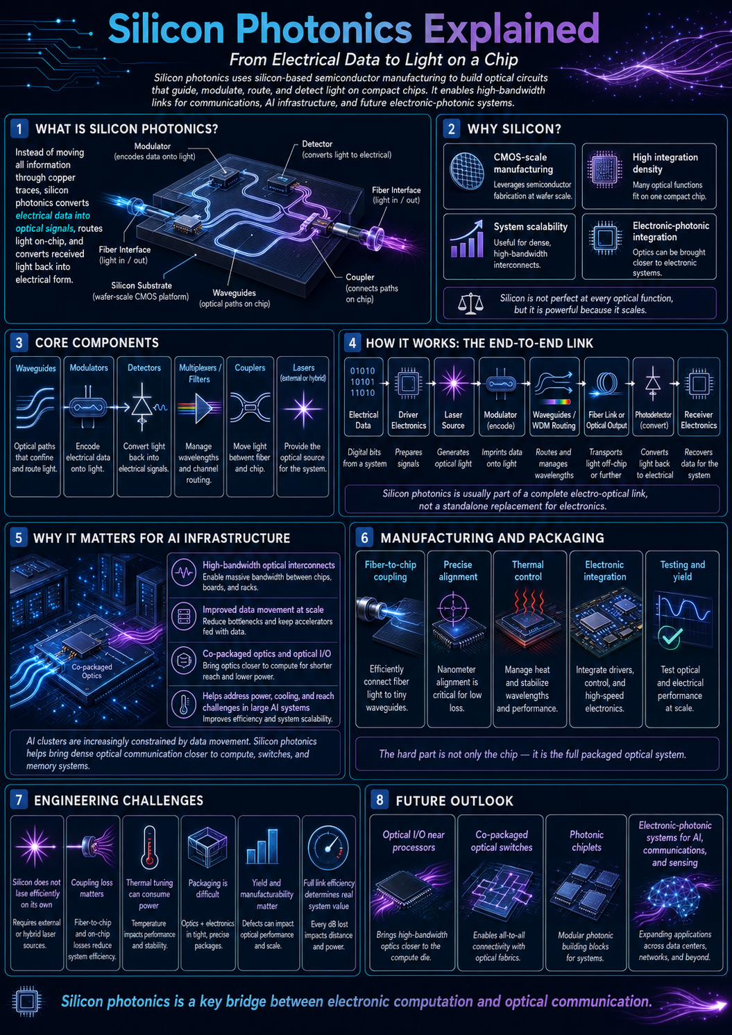
Silicon photonics uses semiconductor manufacturing methods to build optical circuits on silicon-based platforms. It is one of the most important paths for bringing light onto chips and scaling high-bandwidth optical systems for data centers, AI infrastructure, communications, sensing, and future electronic-photonic integration.
Laser InputModulatorWaveguidesDetector
Silicon Photonics at a Glance
This study graphic summarizes the full silicon photonics lesson: how electrical data becomes light on a chip, why silicon matters, which components make the system work, and why packaging determines commercial performance.
Offer this as a downloadable silicon photonics study reference.
Connect this form to your email platform and send visitors the full-size Silicon Photonics infographic. This keeps the page educational while turning the visual reference into a lead magnet.
Silicon photonics brings optical communication onto semiconductor platforms.
Silicon photonics is the field of building photonic integrated circuits using silicon-based manufacturing methods. Instead of moving information only through copper traces and electrical signals, silicon photonics routes light through waveguides, modulators, couplers, filters, and detectors on chip-scale platforms.
The core promise is not that silicon photonics replaces electronic chips. The promise is that optical communication can be integrated closer to electronic systems, creating a pathway toward higher bandwidth density, lower data-movement energy in the right regimes, compact optical engines, and scalable electronic-photonic systems.
Silicon photonics matters because AI infrastructure, cloud networks, and high-performance computing increasingly need more bandwidth than electrical interconnects alone can comfortably provide.
Silicon photonics uses light on silicon-based chips.
A silicon photonic chip is not a normal processor that computes with light. In most commercial systems, it is an optical communication platform. It helps convert electrical data into optical signals, route those optical signals through waveguides, and convert received light back into electrical signals.
Silicon photonics usually combines optical components with electronic control and packaging. The optical layer handles light. The electronic layer drives, detects, controls, calibrates, and processes signals.
Waveguides and optical paths
Light is guided through chip-scale paths instead of through large free-space optics.
Drivers and control circuits
Electronics modulates, detects, tunes, and stabilizes the photonic system.
Fiber, lasers, and coupling
The chip must connect efficiently to fibers, lasers, electrical I/O, and thermal systems.
Silicon is attractive because the semiconductor industry already knows how to scale it.
Silicon became the foundation of electronics because it can be manufactured with enormous precision at wafer scale. Silicon photonics tries to use that manufacturing base to scale optical systems.
The benefit is not that silicon is perfect for every optical function. In fact, silicon has serious limitations. The benefit is that silicon processing, wafer-scale fabrication, packaging ecosystems, and electronic integration create a powerful starting point.
| Why Silicon Helps | Why Silicon Is Difficult |
|---|---|
| Semiconductor manufacturing scale Silicon processes can support repeatable wafer-level fabrication. |
Silicon is not an efficient light emitter Silicon has an indirect bandgap, making laser integration difficult. |
| Compact integration Optical circuits can be made smaller and more stable than bulk optical systems. |
Thermal sensitivity Silicon photonic devices can drift with temperature and require tuning. |
| Electronic compatibility Silicon photonics can be integrated near CMOS electronics and advanced packages. |
Packaging complexity Fiber coupling, laser attachment, and testing are major commercial challenges. |
A silicon photonic system is built from optical building blocks.
Silicon photonic chips combine many optical functions into a compact platform. These components work together to move information between the electrical and optical domains.
Optical wires on a chip
Waveguides confine and route light across the photonic circuit.
Encoding data onto light
Modulators change an optical carrier in response to an electrical signal.
Converting light into current
Detectors receive optical signals and convert photons back into electronic signals.
Connecting chips and fibers
Couplers move light between optical fiber and on-chip waveguides.
Selecting wavelengths
Filters and resonators route, separate, or select optical wavelengths.
Scaling bandwidth
WDM components allow multiple wavelengths to share the same optical path.
The hard part is not only the chip. It is the full packaged system.
Silicon photonics depends on precision manufacturing, but the commercial challenge often extends beyond wafer fabrication. Optical packaging is difficult because tiny misalignments can create large losses.
Silicon photonics is becoming important because AI systems need more data movement.
AI infrastructure is increasingly constrained by bandwidth, power, cooling, and interconnect density. Silicon photonics can help by enabling compact optical interconnects, optical I/O, co-packaged optics, and high-bandwidth links between switches, servers, accelerators, racks, and data centers.
Moving data farther
Optical links can maintain signal quality over distances where high-speed copper becomes difficult.
Moving optics closer
Silicon photonic engines can move closer to switch ASICs and future compute systems.
More data per space
Wavelength multiplexing allows multiple optical channels to share one fiber or waveguide.
Silicon photonics is powerful, but it is not easy.
A credible explanation has to include the constraints. Silicon photonics can improve system architecture, but only when the complete optical link is efficient, manufacturable, and reliable.
Silicon does not lase efficiently
Because silicon has an indirect bandgap, many systems rely on external lasers, III-V integration, or heterogeneous laser strategies.
Loss can erase the advantage
Coupling loss, insertion loss, propagation loss, and detector inefficiency can reduce system performance.
Thermal drift matters
Silicon photonic components can shift with temperature, requiring tuning and control.
Packaging drives cost
Commercial success depends on reliable optical packaging, testing, serviceability, and yield.
Silicon photonics succeeds when the full system works: chip design, laser strategy, coupling, electronics, packaging, thermal control, and manufacturing yield.
Silicon photonics is a bridge between electronic chips and optical systems.
The future of computing and communications will not be purely electronic or purely photonic. It will be electronic-photonic. Silicon photonics is one of the most important platforms for making that integration practical.
Future systems may include optical I/O near processors, photonic chiplets, co-packaged optical switches, silicon photonic transceivers, remote laser sources, and high-bandwidth optical fabrics for AI infrastructure.
Silicon photonics, explained clearly.
What is silicon photonics?
Silicon photonics uses silicon-based semiconductor manufacturing methods to build optical circuits that guide, modulate, route, and detect light on chip-scale platforms.
Why is silicon used for photonics?
Silicon is attractive because it benefits from semiconductor manufacturing scale, compact integration, and compatibility with electronic systems. However, silicon is not an efficient native light emitter.
What is a silicon photonic chip used for?
Silicon photonic chips are commonly used for optical communication, data-center interconnects, optical transceivers, sensing, and emerging optical I/O architectures.
Does silicon photonics replace electronics?
No. Silicon photonics usually works with electronics. Electronics handles logic, control, and signal processing, while photonics handles high-bandwidth optical data movement.
Why does silicon photonics matter for AI?
AI systems need massive data movement. Silicon photonics can help support high-bandwidth, energy-aware optical interconnects and future co-packaged optical systems.
What are the biggest challenges?
The biggest challenges include laser integration, coupling loss, thermal drift, packaging, testing, manufacturing yield, and long-term reliability.