Photonics and AI Infrastructure
A Technical Guide to Optical Interconnects, Silicon Photonics, Co-Packaged Optics, Energy Efficiency, Cooling, and the Future of AI Data Centers
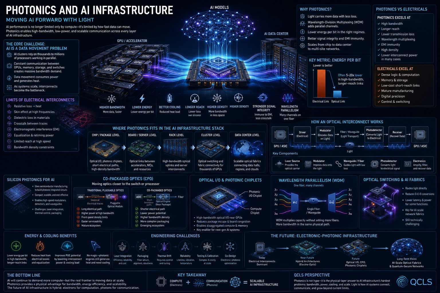
Click to enlarge technical visual
AI Infrastructure at a Glance
This visual reference connects the core engineering ideas: AI data movement, optical interconnects, silicon photonics, co-packaged optics, energy per bit, cooling pressure, and electronic-photonic system design.
Download the full-size QCLS technical reference
Use this as the standard lead-capture area across the QCLS Learning Center. The on-page infographic teaches immediately; the full-size downloadable version builds the email list.
Artificial intelligence is usually described as a compute revolution. At infrastructure scale, however, AI becomes a data movement problem. Artificial intelligence is pushing data centers toward the limits of bandwidth, power, cooling, and data movement. Photonics brings light into AI infrastructure, enabling faster, denser, and more efficient communication between chips, servers, racks, and data centers.
Modern AI systems do not rely on a single processor doing isolated work. They rely on enormous distributed systems made of GPUs, CPUs, AI accelerators, high-bandwidth memory, storage systems, network switches, optical transceivers, power delivery infrastructure, cooling systems, and software orchestration layers. These components must exchange massive amounts of data continuously.
As models become larger and clusters become more complex, the limiting factor is no longer only how many operations a chip can perform. It is how efficiently the entire infrastructure can move information.
That is where photonics becomes important.
Photonics is the science and engineering of using light to transmit, route, modulate, detect, and process information. In AI infrastructure, photonics matters because light can carry data at extremely high bandwidth, over distance, with wavelength-level parallelism, strong signal integrity, and lower transmission loss than many high-speed electrical interconnects.
The serious engineering thesis is simple:
AI scaling is increasingly constrained by bandwidth, power, cooling, and interconnect density. Photonics gives AI infrastructure a way to move more data with better efficiency than electronics alone.
The future of AI infrastructure will not be purely electronic. It will be electronic-photonic.
AI needs compute. But compute needs communication. Photonics is how communication scales.
Executive Technical Summary
AI infrastructure depends on large-scale data movement between compute, memory, storage, and networking systems. As AI clusters scale from thousands to potentially millions of accelerators, electrical interconnects face growing challenges in power consumption, signal integrity, thermal density, reach, and bandwidth density.
Photonics helps address these problems by replacing or supplementing high-speed electrical links with optical links. Optical communication uses photons instead of electrons to carry information through fiber, waveguides, and photonic integrated circuits.
Photonics is already central to long-distance telecommunications and data-center networking. The next step is moving photonics closer to the compute layer through silicon photonics, optical I/O, co-packaged optics, photonic chiplets, and optical interconnect fabrics.
Recent industry and technical research increasingly identifies photonics as a major scaling technology for AI data centers because of its bandwidth, energy efficiency, and scalability across multiple layers of data-center architecture. A 2026 Nature industry analysis described photonics as a transformative solution for AI data centers, specifically citing bandwidth, energy efficiency, and scalability across the AI data-center stack.
Photonics provides AI infrastructure with several engineering advantages:
- Higher bandwidth density
Light can carry high data rates through compact optical channels, and wavelength-division multiplexing allows many optical channels to share the same fiber or waveguide. - Lower loss over distance
Optical fiber and optical waveguides can carry high-speed signals with lower distance-related loss than many high-speed copper interconnects. - Lower energy pressure in data movement
Optical links can reduce the energy required to move data across certain distances and bandwidth regimes. - Reduced cooling burden in interconnect-heavy systems
Photonics does not eliminate heat, but it can reduce some heat generated by high-speed electrical transmission and signal conditioning. - Improved signal integrity
Optical links avoid many electrical signal-integrity problems such as electromagnetic interference, crosstalk, skin effect, and severe high-frequency copper attenuation. - Better reach and scalability
Optical links are already proven across long-haul, metro, data-center, and rack-scale communication. - Pathway to co-packaged optics and optical I/O
Moving optics closer to ASICs, switches, GPUs, and accelerators can reduce electrical trace length and improve system-level bandwidth density.
The important caveat is that photonics is not a universal replacement for electronics. Electronics remains superior for dense logic, memory, control, switching, and arithmetic. Photonics is strongest where the problem is moving information, not necessarily storing or digitally processing it.
The likely future is not “photonic computers replace electronic computers.” The likely future is:
Electronic compute + photonic data movement + electronic-photonic packaging + optical networking.
Why AI Infrastructure Needs a New Data Movement Layer
AI systems are built on parallelism. Training a large model requires many processors working together, sharing parameters, gradients, activations, embeddings, weights, and intermediate results. Inference at scale also requires high-speed movement between memory, accelerators, servers, and networking systems.
The larger the AI system becomes, the more communication dominates performance.
In many AI workloads, compute units spend part of their time waiting for data. When accelerators are underfed, expensive compute hardware is not fully utilized. That means the infrastructure problem is not only “more chips.” It is also:
- more bandwidth
- lower latency
- better synchronization
- higher network utilization
- lower energy per bit
- better cooling efficiency
- less signal loss
- higher interconnect density
- more scalable communication fabrics
The core issue is that AI scaling increases the burden on interconnects.
A simplified AI cluster contains:
GPU / AI Accelerator
      ↓
Package-level interconnect
      ↓
Board-level communication
      ↓
Server network interface
      ↓
Top-of-rack switch
      ↓
Cluster switch fabric
      ↓
Storage / memory / other accelerators
      ↓
Another GPU / AI accelerator
Every layer consumes power, adds latency, creates heat, and introduces potential bottlenecks.
At small scale, electrical interconnects are sufficient. At very large scale, the physical limits of electrical data movement become more obvious.
The Electrical Interconnect Problem
Electrical interconnects move data using electrons and electromagnetic signals through conductive materials such as copper traces, cables, package substrates, printed circuit boards, and interposers.
Electronics is excellent for computation and control. But high-speed electrical data movement faces several hard engineering constraints.
1. Resistive Loss
Copper is conductive, but it is not perfect. Electrical signals lose energy as heat through resistance. As frequency rises and interconnects become denser, resistive losses become more significant.
This heat must be removed by the cooling system.
2. Skin Effect
At high frequencies, current tends to flow near the surface of a conductor. This reduces the effective conducting area and increases resistance.
For high-speed AI interconnects, skin effect contributes to signal attenuation and energy loss.
3. Dielectric Loss
Signals traveling through printed circuit boards, packages, and cables interact with dielectric materials. At high data rates, dielectric losses can become significant.
This limits reach and increases the need for equalization, retiming, and signal conditioning.
4. Crosstalk
Dense electrical traces can interfere with one another. As interconnect density increases, crosstalk becomes harder to manage.
Crosstalk degrades signal integrity and can increase error rates.
5. Electromagnetic Interference
Electrical signals are susceptible to electromagnetic interference. Shielding and careful layout can reduce the problem, but at high speeds and high densities, electromagnetic interactions become increasingly difficult.
6. Equalization and Retiming Power
As electrical links become faster and longer, the receiver often requires equalization, clock recovery, retiming, and digital signal processing to reconstruct the transmitted data.
These circuits consume power.
In other words, electrical links do not only consume power in the wire. They also consume power in the circuitry required to make the signal usable after transmission.
7. Bandwidth Density Limits
Modern AI systems need huge bandwidth through limited physical space. Package edges, board routing channels, switch faceplates, and rack-level connections all create physical bottlenecks.
If the system cannot physically route enough high-speed electrical signals, scaling becomes difficult even if compute chips keep improving.
Why Photonics Fits the AI Infrastructure Problem
Photonics fits because AI infrastructure increasingly needs to move enormous quantities of data through constrained physical space with lower energy and better reach.
Optical communication uses light instead of electrical current as the carrier.
A simplified optical interconnect works like this:
Electrical data
      ↓
Driver circuit
      ↓
Laser or optical carrier
      ↓
Modulator encodes data onto light
      ↓
Fiber or waveguide transports optical signal
      ↓
Photodetector converts light back to electrical signal
      ↓
Receiver electronics recover data
The advantage is not magic. It is physics.
Photons do not experience electrical resistance in the same way electrons do in metal conductors. Optical fibers can carry high-bandwidth signals over long distances with low loss. Optical channels can use multiple wavelengths simultaneously. Optical links are not affected by electromagnetic interference in the same way copper links are.
This is why optical communication already dominates long-distance data transmission.
The next question is: How close can optics move toward the processor?
That is the frontier of AI photonics.
Photonics vs Copper: Where Light Has the Advantage
Photonics is not always better than copper. Copper is cheap, mature, and excellent over short distances. Electronics is still dominant inside chips and packages.
But as distance, bandwidth, and density increase, optical links become more attractive.
Copper Is Strongest When:
- distances are very short
- bandwidth requirements are moderate
- cost sensitivity is high
- integration with electronic circuits is simple
- power and thermal constraints are manageable
- the interconnect is inside a chip or package
Photonics Is Strongest When:
- bandwidth requirements are very high
- distance increases
- signal integrity becomes difficult
- power per bit becomes critical
- cooling becomes limiting
- many parallel data channels are needed
- electromagnetic interference matters
- bandwidth density becomes physically constrained
- many systems need to communicate at scale
That is why photonics is becoming more important as AI infrastructure scales.
It is not because light is fashionable. It is because the data movement problem increasingly favors optical physics.
The Key Metric: Energy Per Bit
One of the most important metrics in AI infrastructure is energy per bit.
Energy per bit measures how much energy is required to move one bit of information.
Energy per bit = total link energy / number of bits transmittedThis is critical because AI systems move extraordinary amounts of data. Even small improvements in energy per bit can matter at data-center scale.
If a data center moves exabits of information, energy per bit becomes a major part of total power consumption.
Electrical interconnects consume energy through:
- driver circuits
- receiver circuits
- resistance
- equalization
- retiming
- clocking
- signal conditioning
- thermal overhead
- power delivery losses
Optical interconnects consume energy through:
- lasers
- modulators
- drivers
- detectors
- receiver electronics
- thermal tuning
- control circuits
- packaging overhead
Photonics is not energy-free. But in the right regimes, optical links can reduce the energy required for high-bandwidth data movement, especially as distance and bandwidth scale.
This is why photonics is important for AI cooling: not because it eliminates heat, but because it can reduce energy wasted in data movement.
Cooling: Why Photonics Matters Thermally
AI data centers are increasingly power-limited and cooling-limited. More compute generates more heat. More memory bandwidth generates more heat. More networking generates more heat. More electrical signal conditioning generates more heat.
Cooling is not a side issue. It is now part of AI system architecture.
Photonics can help reduce cooling pressure in the interconnect layer.
The key point is this:
Photonics does not make AI infrastructure heat-free. It makes high-bandwidth data movement more thermally scalable.
Optical interconnects can help reduce:
- resistive heating in long high-speed electrical paths
- power required for electrical equalization
- thermal load from dense electrical I/O
- signal-conditioning overhead at high speeds
- package and board-level electrical congestion
However, photonic systems still generate heat from lasers, modulators, drivers, detectors, thermal tuning circuits, and control electronics.
The correct engineering view is balanced:
Photonics reduces certain thermal bottlenecks while introducing its own packaging, laser, and thermal-control challenges.
That is why electronic-photonic co-design is so important.
Bandwidth Density: Why AI Needs More Than Faster Lanes
AI infrastructure needs more than higher per-lane data rates. It needs more total bandwidth through limited physical space.
Bandwidth density measures how much data throughput can be achieved per unit area, per package edge, per board footprint, per rack unit, or per watt.
Photonics helps bandwidth density in three ways.
1. High-Speed Optical Channels
Optical links can support very high data rates per channel.
2. Wavelength-Division Multiplexing
Multiple wavelengths of light can travel through the same fiber or waveguide at the same time. This is called wavelength-division multiplexing, or WDM.
Instead of requiring one physical conductor per channel, optical systems can multiplex many channels onto one optical path.
3. Compact Optical Routing
Integrated photonics can route optical signals through waveguides on chips or packages, allowing compact optical engines, transceivers, and interconnect systems.
The result is a path toward moving more data through less physical space.
That matters because AI systems are increasingly constrained by package escape, switch radix, rack density, faceplate bandwidth, and board routing.
Wavelength-Division Multiplexing: Photonics’ Parallelism Advantage
One of the strongest scientific advantages of photonics is wavelength parallelism.
Light can be separated by wavelength. Different wavelengths can carry different streams of data simultaneously through the same optical fiber or waveguide.
This is wavelength-division multiplexing.
A simplified WDM system looks like this:
λ1 → data channel 1
λ2 → data channel 2
λ3 → data channel 3
λ4 → data channel 4
λ5 → data channel 5
All wavelengths travel through the same fiber.
This is powerful because bandwidth can scale by adding wavelengths.
Electronics generally scales bandwidth by increasing signaling rate, adding lanes, improving encoding, reducing noise, and using more complex equalization. Photonics can also increase lane speed, but it has the additional advantage of wavelength parallelism.
For AI infrastructure, WDM can support:
- higher fiber capacity
- denser optical links
- more aggregate bandwidth
- reduced cable complexity
- more scalable interconnect fabrics
This does not make WDM trivial. It requires lasers, wavelength control, multiplexers, demultiplexers, thermal stability, filters, and precise optical design.
But it gives photonics a unique scaling dimension.
Optical Interconnects for AI
An optical interconnect is a communication link that uses light to move information between system components.
In AI infrastructure, optical interconnects can exist at multiple levels:
1. Data Center Interconnect
This connects data centers or large facilities over long distances.
Photonics already dominates here.
2. Cluster Interconnect
This connects groups of servers, racks, and switches inside an AI data center.
Optics is already widely used here through transceivers and fiber links.
3. Rack-Level Interconnect
This connects servers and switches within racks or between nearby racks.
Optical links become more attractive as bandwidth increases.
4. Board-Level Interconnect
This connects components inside servers or accelerator systems.
This is an emerging frontier.
5. Chip-to-Chip Interconnect
This connects processors, accelerators, memory, and chiplets.
This is one of the hardest and most important future frontiers.
6. On-Package Optical I/O
This places optical engines very close to ASICs, GPUs, or accelerators.
This is where integrated photonics and advanced packaging become critical.
Silicon Photonics for AI Infrastructure
Silicon photonics uses silicon-based semiconductor manufacturing methods to build photonic integrated circuits.
It matters for AI infrastructure because it can potentially combine:
- optical communication performance
- semiconductor manufacturing scale
- compact integration
- lower-cost wafer-level production
- compatibility with electronic systems
- dense optical I/O
- integrated modulators and detectors
Silicon photonics is used in optical transceivers, data-center interconnects, coherent optics, sensing, and emerging optical I/O architectures.
A major industry issue is that silicon is not an efficient native light emitter. Silicon has an indirect bandgap, which makes laser integration difficult. As a result, silicon photonic systems often use external lasers, hybrid III-V integration, heterogeneous integration, or co-packaged light sources.
That is why silicon photonics is not only a photonic design challenge. It is a packaging, materials, and manufacturing challenge.
A 2026 Semiconductor Engineering analysis notes that photonic interconnects can increase bandwidth density while reducing power consumption, but also highlights material compatibility, thermal, and mechanical stress challenges.
This is the realistic view: silicon photonics is powerful, but commercialization depends on solving manufacturing and packaging problems.
Co-Packaged Optics: Moving Light Closer to Compute
Co-packaged optics, or CPO, is one of the most important ideas in AI photonics.
Traditional optical networking often uses pluggable optical modules at the front panel of a switch. Electrical signals travel from the switch ASIC across the board to the pluggable module, where they are converted into optical signals.
As bandwidth rises, that electrical path becomes more power-hungry and difficult.
Co-packaged optics moves optical engines closer to the switch ASIC or compute package.
The goal is to reduce the distance high-speed electrical signals must travel before optical conversion.
Traditional Pluggable Optics
ASIC → long electrical board trace → pluggable optical module → fiberCo-Packaged Optics
ASIC → short electrical connection → optical engine near package → fiberThe advantage is that shorter electrical paths can reduce signal loss, lower power consumption, and improve bandwidth density.
NVIDIA has publicly described co-packaged optics as a way to improve power efficiency and resiliency for large-scale AI factories. Yole Group has also described co-packaged optics as an emerging critical technology for addressing AI-driven bandwidth and energy challenges.
This does not mean CPO is easy. It introduces challenges in:
- serviceability
- thermal management
- optical coupling
- laser reliability
- fiber attach
- manufacturing yield
- testing
- field repair
- supply chain maturity
- standardization
But the direction is clear: as AI systems scale, optics is moving closer to compute and switching silicon.
Pluggable Optics vs Co-Packaged Optics
Both architectures matter.
Pluggable Optics
Advantages:
- mature ecosystem
- easier service and replacement
- established supply chain
- modular upgrades
- lower integration risk
- widely deployed
Limitations:
- longer electrical reach from ASIC to module
- higher power at very high bandwidth
- faceplate density limits
- signal integrity challenges
- scaling pressure as switch bandwidth rises
Co-Packaged Optics
Advantages:
- shorter electrical paths
- higher bandwidth density potential
- lower power potential
- better scaling for large switches
- closer integration with AI network fabrics
Limitations:
- harder serviceability
- complex packaging
- thermal challenges
- laser integration and reliability concerns
- more difficult testing
- less mature ecosystem
The likely future is not instant replacement. It is a transition where pluggable optics, linear-drive optics, near-packaged optics, and co-packaged optics coexist depending on the system requirement.
Optical I/O: The Next Step Toward Chip-Level Photonics
Optical I/O means using optical links for input/output near chips, packages, or accelerator systems.
This matters because AI accelerators need to move enormous amounts of data off-chip. Package-level and board-level I/O are becoming bottlenecks.
Electrical I/O faces limits in:
- power
- reach
- bandwidth density
- package escape
- signal integrity
- thermal load
Optical I/O offers a way to move data with high bandwidth and lower distance-related loss.
The long-term direction is:
GPU / AI accelerator
      ↓
short electrical path
      ↓
photonic I/O engine
      ↓
fiber or optical waveguide
      ↓
remote accelerator / switch / memory system
This could help enable:
- larger AI clusters
- disaggregated compute
- memory pooling
- accelerator-to-accelerator links
- lower-power scale-out networks
- chiplet-level photonic connectivity
Research and industry development are moving toward tighter integration of electronics and photonics. Columbia Engineering reported a 3D photonic-electronic platform in 2025 aimed at high bandwidth density and energy efficiency for next-generation AI hardware.
Photonic Chiplets and Advanced Packaging
A chiplet is a small functional die integrated with other dies in an advanced package. The semiconductor industry is increasingly moving toward chiplet architectures because monolithic scaling is becoming more difficult and expensive.
Photonic chiplets could provide optical communication functions inside advanced packages.
A future AI package might include:
- compute chiplets
- memory chiplets
- electronic I/O chiplets
- photonic I/O chiplets
- optical engines
- interposers
- fiber attach
- power delivery
- thermal management
The photonic chiplet would handle high-bandwidth optical communication while electronic chiplets handle computation and control.
This is one of the most important long-term possibilities for AI infrastructure.
Optical Switching and AI Network Fabrics
Today’s AI networks often rely heavily on electronic switching. Optical signals are converted into electrical signals, switched electronically, and sometimes converted back into optical signals.
That optical-electrical-optical conversion can add power, latency, and complexity.
Optical switching aims to route light more directly.
Potential advantages include:
- lower power for some switching functions
- reduced conversions
- high bandwidth
- lower latency
- scalable optical paths
- better support for large cluster fabrics
However, optical switching has challenges:
- switching speed
- control plane complexity
- loss
- wavelength management
- buffering limitations
- integration with packet-based networks
- reliability
- cost
Optical switching may become important in AI-scale networks, but it is not a simple replacement for electronic switching. It will likely appear in specific layers where optical circuit switching or hybrid packet/circuit architectures make sense.
Photonics for AI Infrastructure vs Photonic Computing
This distinction is extremely important.
Photonics for AI Infrastructure
This means using light to move data in and around AI systems.
Examples:
- optical transceivers
- silicon photonics
- co-packaged optics
- optical I/O
- optical interconnects
- optical switching
- data-center fiber networks
This is already commercially important and likely to grow rapidly.
Photonic Computing
This means using light to perform computation itself.
Examples:
- optical matrix multiplication
- photonic neural networks
- analog optical processors
- diffractive optical computing
- interferometer mesh processors
- reservoir computing
- optical accelerators
Photonic computing is promising, especially for certain linear algebra and signal-processing operations, but it has different challenges:
- precision
- noise
- programmability
- nonlinear activation
- memory integration
- analog-to-digital conversion
- software ecosystem
- training compatibility
- manufacturing variation
- calibration
The near-term AI infrastructure opportunity is stronger and more immediate than fully replacing digital electronic computation.
In simple terms:
Photonics will likely enter AI first as a data movement technology, then selectively as a computing acceleration technology.
That is the serious, non-hype version.
Why Photonics Can Beat Electronics in AI Data Movement
Photonics has strong advantages in specific regimes. The key is to compare by function, not by ideology.
1. Speed and Bandwidth
Optical carriers operate at extremely high frequencies. More importantly, photonics supports wavelength parallelism. Multiple wavelengths can carry independent data streams through the same physical channel.
This makes photonics extremely strong for high-bandwidth communication.
2. Distance Scaling
Electrical links degrade rapidly at high speeds over distance. Optical links can maintain signal integrity over longer distances with lower loss.
That is why fiber is used for long-distance communication and why optics becomes increasingly attractive as AI clusters scale across racks and facilities.
3. Lower Transmission Loss
Optical channels can have lower distance-related transmission loss than copper links in high-speed regimes. This helps reduce the need for heavy electrical equalization and signal conditioning.
4. Better Electromagnetic Isolation
Photons are electrically neutral. Optical fibers do not radiate or pick up electromagnetic interference like copper conductors.
This improves signal integrity and reduces crosstalk problems.
5. Wavelength Multiplexing
WDM gives photonics a unique parallel scaling mechanism.
A single fiber can carry many wavelengths. Each wavelength can carry high-speed data. This is a powerful bandwidth multiplier.
6. Cooling Advantage in Interconnects
Photonics reduces some heat associated with electrical data movement. This matters when interconnect power becomes a large part of system power.
7. Physical Infrastructure Compatibility
Optical fiber is already widely deployed in telecommunications and data centers. Photonics builds on a mature communication foundation.
Where Electronics Still Wins
A credible technical page should say this clearly:
Photonics is not superior everywhere.
Electronics still wins in:
- dense logic
- memory
- transistor switching
- digital control
- arithmetic precision
- cache systems
- register files
- local on-chip communication
- low-cost short-reach interconnects
- mature manufacturing
- software-programmable computation
Photons are excellent for movement and measurement. Electrons are excellent for logic and storage.
That is why the future is hybrid.
The AI Data Center Stack: Where Photonics Adds Value
Facility Layer
At the facility level, photonics supports high-capacity interconnection between data centers, campuses, and cloud regions.
Cluster Layer
At the cluster level, optics connects racks, switches, and groups of servers.
Rack Layer
At the rack layer, optical links can support high-bandwidth communication between AI servers and top-of-rack switches.
Server Layer
At the server layer, optics may increasingly support high-speed connections between accelerators and network interfaces.
Package Layer
At the package layer, optical I/O and photonic chiplets may eventually connect compute dies, switch dies, and accelerator packages.
Chip Layer
Inside the chip, electronics still dominates. But photonic structures may eventually play a role in specialized clocking, optical I/O, or certain analog acceleration functions.
The key architectural direction is that photonics moves closer and closer to the compute engine as bandwidth and power pressures increase.
Practical Example: Why a GPU Cluster Needs Photonics
Imagine an AI training cluster with thousands of accelerators.
Each accelerator performs matrix operations, but it must constantly exchange data with other accelerators. If communication is slow, the accelerators wait. If communication consumes too much power, the system becomes power-limited. If communication creates too much heat, the data center becomes cooling-limited. If the network cannot scale, the cluster cannot efficiently train larger models.
Photonics helps by increasing the capacity and efficiency of the communication layer.
It does not make the GPU itself magically faster. Instead, it helps the whole AI system operate more efficiently by reducing communication bottlenecks.
This is why photonics is infrastructure-level technology.
It improves the system around the compute.
Practical Example: Why Co-Packaged Optics Matters for AI Switches
AI clusters require large switch fabrics. As switch ASIC bandwidth increases, the electrical path from the ASIC to front-panel pluggable optics becomes more difficult.
At very high bandwidths, that electrical path consumes more power and becomes harder to equalize.
Co-packaged optics moves optical engines closer to the ASIC, reducing the electrical distance.
This can improve:
- power efficiency
- bandwidth density
- signal integrity
- faceplate constraints
- network scaling
NVIDIA’s 2025 Spectrum-X Photonics announcement claimed major improvements in power efficiency, signal integrity, resiliency, and deployment compared with traditional methods for large-scale AI networking. Claims from vendors should always be interpreted in context, but the direction supports the broader industry trend: AI networking is pushing optics closer to the switching silicon.
The Role of Lasers in AI Photonics
Lasers are essential because photonic systems need optical carriers.
In optical communication, the laser provides the light. Modulators encode data onto that light. Detectors recover the signal.
Laser architecture is one of the most important design choices.
Options include:
- integrated lasers
- external laser sources
- remote laser sources
- distributed laser architectures
- III-V lasers
- hybrid silicon lasers
- co-packaged lasers
Laser reliability, efficiency, wavelength stability, thermal behavior, and coupling efficiency all affect system performance.
One reason silicon photonics is challenging is that silicon does not naturally make efficient lasers. This forces system designers to solve laser integration through other materials and packaging strategies.
Modulators: Encoding AI Data Onto Light
A modulator converts electrical data into optical data.
It changes the optical carrier in response to an electrical signal.
Common modulation approaches include:
- intensity modulation
- phase modulation
- electro-absorption modulation
- Mach-Zehnder modulation
- ring resonator modulation
- lithium niobate modulation
- silicon carrier-depletion modulation
For AI infrastructure, modulator performance matters because it affects:
- data rate
- power consumption
- signal quality
- footprint
- thermal stability
- drive voltage
- bandwidth density
- integration complexity
A high-performance optical link requires efficient modulators that can operate at high speeds with low energy and acceptable loss.
Photodetectors: Converting Light Back Into Electrical Data
A photodetector receives optical signals and converts them into electrical current.
Detector performance affects:
- receiver sensitivity
- bandwidth
- noise
- link budget
- error rate
- power consumption
- signal integrity
Common detector materials include germanium, indium phosphide, and other III-V semiconductors. In silicon photonics, germanium-on-silicon detectors are widely used because germanium can absorb telecom-band light more effectively than silicon.
The detector is where the optical signal re-enters the electronic system.
This is why electronic-photonic integration is essential. Photonics does not operate in isolation. It must interface cleanly with electronics.
Link Budget: The System-Level Reality
Every optical link has a link budget.
The link budget accounts for gains and losses from source to receiver.
Losses may come from:
- laser coupling
- modulator insertion loss
- waveguide propagation loss
- splitter loss
- bend loss
- fiber coupling loss
- connector loss
- filter loss
- detector coupling loss
- aging
- temperature drift
- manufacturing variation
A simplified link budget must ensure:
Received optical power > receiver sensitivity + system marginIf the link budget is poor, the system may need more laser power, better detectors, lower-loss components, or stronger signal processing.
This matters for AI infrastructure because power is precious. A photonic system with poor coupling and high loss may lose its energy advantage.
That is why packaging and coupling are not minor details. They are central to whether AI photonics works commercially.
Packaging: The Hard Part Nobody Should Ignore
In photonics, packaging is often harder than the chip.
A photonic chip can perform well in a lab, but commercial deployment requires stable, manufacturable, reliable packaging.
Photonics packaging must manage:
- fiber alignment
- optical coupling
- laser integration
- electrical I/O
- thermal control
- mechanical stress
- vibration
- contamination
- serviceability
- high-volume manufacturing
- testing and calibration
- long-term reliability
For AI infrastructure, packaging is especially difficult because systems require high density, high reliability, low cost, and field serviceability.
This is one reason adoption takes time. The physics is strong, but the engineering must be solved at scale.
Thermal Drift in Photonic Systems
Photonics can reduce some thermal problems, but photonic devices can also be temperature-sensitive.
For example, ring resonators and interferometers can shift their behavior as temperature changes. A small temperature shift can move a resonance wavelength, affecting filtering or modulation.
This creates a control problem.
Thermal drift may require:
- heaters
- temperature sensors
- feedback loops
- calibration
- athermal design
- material engineering
- active tuning
In dense AI systems, thermal drift is a serious issue because data centers are already thermally stressed.
This is why “photonics solves cooling” is too simplistic.
A better statement is:
Photonics can reduce interconnect-related heat, but dense photonic systems still require careful thermal engineering.
Reliability and Serviceability
AI infrastructure requires high uptime.
A photonic system must be reliable under real operating conditions, not only impressive in a laboratory.
Important reliability questions include:
- How long do the lasers last?
- What happens when an optical engine fails?
- Can the system be serviced in the field?
- Can fibers be attached reliably at scale?
- How does thermal cycling affect alignment?
- How does packaging stress affect coupling?
- Can optical engines be tested economically?
- Can manufacturing yield support data-center scale?
These questions determine whether a technology becomes infrastructure.
Security Benefits of Photonics in AI Infrastructure
Photonics can contribute to security, but again, precision matters.
Fiber Physical Security
Optical fiber can be monitored for disturbances, bending, tapping, or intrusion. Fiber sensing can detect changes along the fiber path.
Electromagnetic Isolation
Optical fiber does not radiate electromagnetic signals like copper conductors. This can reduce some electromagnetic leakage risks and improve isolation.
Quantum Communication
Photonics is essential to quantum communication and quantum key distribution. However, QKD is not a universal replacement for cryptography. It has practical limitations related to distance, authentication, trusted nodes, hardware security, cost, and integration.
Secure Timing and Sensing
Photonic systems can support secure time transfer, precision sensing, and infrastructure monitoring.
The strongest near-term security benefit for AI infrastructure is probably not “quantum encryption everywhere.” It is physical-layer integrity, electromagnetic isolation, high-quality fiber infrastructure, and eventually specialized quantum-secure links where justified.
The Engineering Benefits of Photonics Over Other Technologies
Photonics competes and cooperates with several technologies: copper interconnects, wireless links, electronic switching, and conventional pluggable optics.
Photonics vs Copper
Photonics wins in high-bandwidth, longer-reach, high-density, signal-integrity-sensitive environments.
Copper wins in short-reach, low-cost, mature, highly integrated environments.
Photonics vs Wireless
Photonics wins in bandwidth, latency, reliability, security, and controlled infrastructure.
Wireless wins in mobility and deployment flexibility.
AI data centers need deterministic, high-capacity, low-latency communication. That strongly favors fiber and photonic links over wireless.
Co-Packaged Optics vs Pluggable Optics
CPO can improve power and bandwidth density by moving optics closer to ASICs.
Pluggable optics remains easier to service and more mature.
The transition will be workload- and architecture-dependent.
Photonics vs Purely Electronic Scaling
Electronic scaling is still essential, but interconnect power and bandwidth are increasingly limiting. Photonics offers a different scaling path: use light for data movement instead of forcing copper and electrical I/O to handle every layer of communication.
What Photonics Does Not Solve
To stay credible, it is important to explain what photonics does not solve.
Photonics does not automatically solve:
- GPU compute efficiency
- memory capacity
- software bottlenecks
- model architecture inefficiency
- data pipeline problems
- power delivery constraints
- facility-level cooling by itself
- semiconductor manufacturing cost
- all network congestion
- all latency problems
- cybersecurity by default
Photonics is a powerful infrastructure technology, but it must be integrated into a full system architecture.
The correct claim is not:
Photonics solves AI.
The correct claim is:
Photonics helps solve one of AI infrastructure’s hardest problems: scalable, high-bandwidth, energy-efficient data movement.
That is a much stronger and more credible position.
The Future of AI Infrastructure Is Electronic-Photonic
AI infrastructure is moving toward systems where electronics and photonics are co-designed.
Future systems may include:
- GPUs with optical I/O
- photonic chiplets
- co-packaged optical switches
- silicon photonic transceivers
- optical circuit switching
- AI-scale optical fabrics
- remote laser sources
- integrated optical engines
- photonic-electronic interposers
- disaggregated memory over optical links
- multi-data-center AI training links
- quantum-secure optical channels for specialized use cases
The architecture may evolve from:
Compute chip → electrical board → pluggable optics → fiberToward:
Compute chip → photonic I/O → optical fabric → compute/memory/network resourceThat transition is technically difficult, but it is the direction the physics and infrastructure pressures point toward.
QCLS Perspective: Why Photonics Matters for AI
AI is not only a software revolution. It is an infrastructure revolution.
The next generation of AI depends on the ability to move data faster, farther, denser, and more efficiently. Compute chips will continue to improve, but the systems around them must also evolve.
Photonics matters because it addresses the interconnect problem at the physical layer.
Light can carry enormous bandwidth.
Light can travel through fiber with low loss.
Light can support many wavelengths in parallel.
Light avoids many electrical signal-integrity problems.
Light can reduce data-movement energy in the right regimes.
Light can help AI infrastructure scale beyond what copper alone can support.
This is why photonics is becoming foundational to AI data centers, optical interconnects, co-packaged optics, silicon photonics, and next-generation computing infrastructure.
The serious version is simple:
AI needs compute. But compute needs communication. Photonics is how communication scales.
Photonics and AI Infrastructure FAQ
Why does AI infrastructure need photonics?
AI infrastructure needs photonics because large AI systems require massive high-speed data movement between accelerators, memory, switches, servers, and data centers. Photonics can help improve bandwidth density, reduce distance-related signal loss, and lower energy pressure in high-bandwidth communication links.
Is photonics faster than electronics?
Photonics can support extremely high-bandwidth communication and wavelength-level parallelism, making it superior for many data movement tasks. Electronics remains superior for dense logic, memory, and digital control.
How does photonics reduce cooling pressure?
Photonics can reduce some heat associated with high-speed electrical data movement by lowering transmission losses and reducing the need for power-hungry electrical signal conditioning in certain links. However, photonic systems still generate heat through lasers, modulators, detectors, and control electronics.
What is co-packaged optics?
Co-packaged optics places optical engines close to switch ASICs or processors instead of relying only on pluggable optical modules at the front panel. This can shorten high-speed electrical paths and improve bandwidth density and power efficiency.
What is silicon photonics?
Silicon photonics uses silicon-based semiconductor manufacturing techniques to build optical circuits. It enables compact photonic integrated circuits for optical communication, data-center interconnects, sensing, and AI infrastructure.
Will photonics replace GPUs?
No. Photonics will not replace GPUs in the near term. GPUs and AI accelerators perform computation, while photonics is most useful for moving data efficiently between compute resources. The future is likely hybrid electronic-photonic infrastructure.
What is optical I/O?
Optical I/O uses optical links for input and output near chips, packages, or accelerator systems. It can help move data with high bandwidth and lower distance-related loss than many electrical links.
Is photonic computing the same as photonics for AI infrastructure?
No. Photonics for AI infrastructure uses light to move data between compute systems. Photonic computing uses light to perform computation itself. Infrastructure applications are more commercially mature today, while photonic computing remains an emerging area.
Integrated Photonics
Technical Guide to Photonic Integrated Circuits, Optical Chips, Waveguides, Silicon Photonics, and Light-Based Systems
Silicon Photonics
Waveguides
Optical I/O
AI Infrastructure
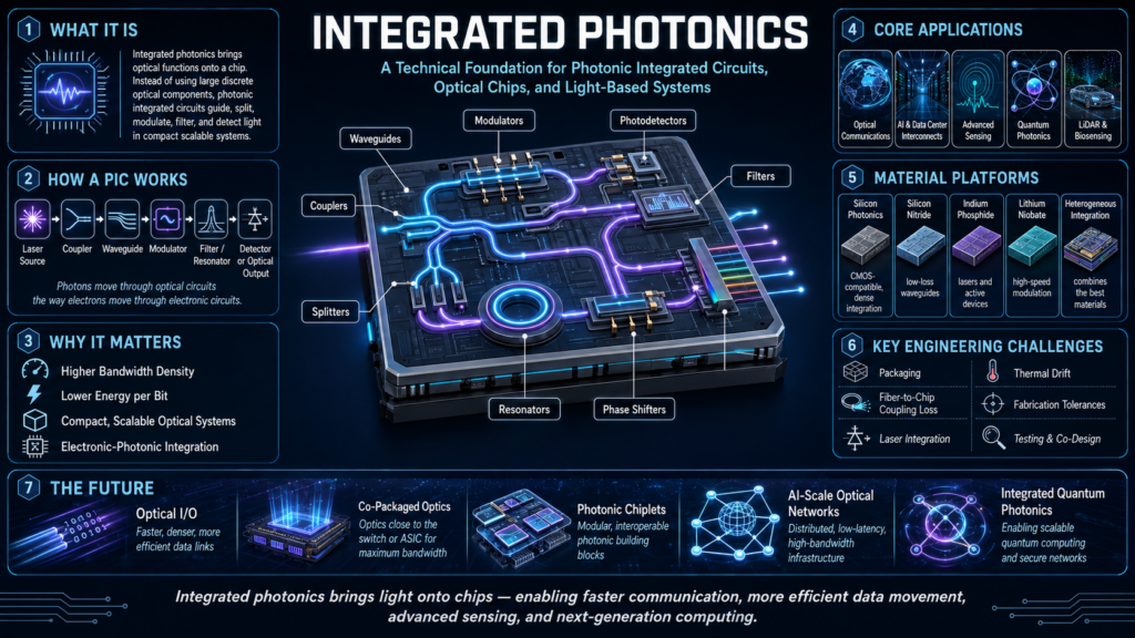
View larger infographic →
Integrated Photonics at a Glance
This full-width infographic turns the page into a visual learning system: what integrated photonics is, how a PIC works, why it matters, material platforms, engineering challenges, and the future of optical I/O, photonic chiplets, and quantum integration.
Want the full-size technical infographic?
Use the on-page image freely for learning. For the downloadable high-resolution version, connect this form to your email platform and send visitors the full-size infographic as a lead magnet.
Core thesis: Integrated photonics brings light onto chips — enabling compact optical systems for high-speed communication, AI infrastructure, advanced sensing, quantum technology, and scalable electronic-photonic architectures.
Integrated Photonics Explained
Integrated photonics is the engineering discipline of building optical systems on chips.
Where electronics uses integrated circuits to route, switch, amplify, and process electrical signals, integrated photonics uses photonic integrated circuits to route, modulate, filter, split, combine, detect, and process light. Instead of moving information only through electrons in metal traces, integrated photonics moves information through photons confined inside optical waveguides.
At a high level, integrated photonics attempts to do for light what microelectronics did for electricity: reduce large, complex systems into compact, manufacturable, chip-scale platforms.
A photonic integrated circuit, often called a PIC, is a microchip containing multiple photonic components that form a functioning optical circuit. These components can include waveguides, modulators, detectors, couplers, filters, resonators, interferometers, multiplexers, optical switches, and light-coupling structures. PhotonDelta describes a PIC as a microchip containing two or more photonic components that form a functioning circuit, using photons rather than electrons to perform optical functions.
Integrated photonics matters because modern technology is increasingly limited by data movement, bandwidth density, power consumption, heat, latency, and signal integrity. As computing, artificial intelligence, cloud infrastructure, quantum systems, telecommunications, and sensing platforms scale, electronic systems alone face growing physical and economic constraints.
Integrated photonics is one of the major engineering paths toward faster, smaller, more efficient, and more scalable optical systems.
Executive Technical Summary
Integrated photonics brings optical components onto a chip-scale platform. Instead of building optical systems from separate lasers, lenses, mirrors, fibers, filters, and detectors, engineers can fabricate multiple optical functions on a substrate using semiconductor-style processes.
A photonic integrated circuit can guide light through waveguides, split and combine optical paths, modulate optical signals, filter wavelengths, detect photons, route signals, and interface with electronic circuits.
The core value of integrated photonics is system-level efficiency.
It can reduce:
- optical system size
- alignment complexity
- power per transmitted bit
- signal loss over high-bandwidth links
- packaging footprint
- manufacturing variability
- cost at scale
- data movement bottlenecks
It can improve:
- bandwidth density
- communication speed
- optical signal integrity
- sensing precision
- scalability
- chip-to-chip and rack-to-rack connectivity
- AI data-center interconnects
- quantum photonic integration
- electronic-photonic co-design
Integrated photonics is especially important for:
- optical communications
- data centers
- AI infrastructure
- photonic integrated circuits
- silicon photonics
- co-packaged optics
- quantum photonics
- LiDAR
- biosensing
- spectroscopy
- optical computing
- advanced sensing
- chip-scale optical systems
The engineering future is not purely electronic or purely photonic. It is hybrid.
The most advanced systems will use electronics for dense digital logic and control, while using photonics for high-bandwidth data movement, optical input/output, precision sensing, quantum communication, and specialized light-based processing.
What Is Integrated Photonics?
Integrated photonics is the miniaturization and integration of optical components onto a chip.
A traditional optical system might include:
- a laser source
- lenses
- mirrors
- filters
- fiber couplers
- modulators
- beam splitters
- detectors
- alignment mounts
- thermal controls
- mechanical stages
- free-space optical paths
That type of system can be powerful, but it is often large, expensive, fragile, alignment-sensitive, and difficult to manufacture at scale.
Integrated photonics replaces many of these discrete components with chip-scale equivalents.
On a photonic chip:
- waveguides replace free-space optical paths
- grating couplers or edge couplers connect fibers to chips
- ring resonators or arrayed waveguide gratings filter wavelengths
- Mach-Zehnder interferometers modulate or switch signals
- photodiodes detect optical signals
- splitters and couplers distribute optical power
- phase shifters tune optical paths
- multiplexers combine wavelength channels
- demultiplexers separate wavelength channels
- electronic drivers and control circuits manage the optical device
This allows complex optical functions to be built into compact, repeatable, manufacturable systems.
Photonic Integrated Circuits: The Core Platform
A photonic integrated circuit is the fundamental hardware platform of integrated photonics.
A PIC is not simply a “chip with light.” It is an engineered optical circuit where light is generated, coupled, guided, split, modulated, filtered, delayed, switched, combined, and detected.
A simplified PIC system may look like this:
Laser source ↓ Fiber-to-chip coupler or integrated laser ↓ Input waveguide ↓ Modulator ↓ Splitter / filter / resonator / interferometer ↓ Multiplexer or routing network ↓ Output coupler or detector ↓ Electronic readout or optical transmissionIn practice, PICs can be much more complex. Advanced photonic circuits may contain hundreds or thousands of optical elements, especially in communication, sensing, optical computing, and quantum photonics applications.
The major engineering challenge is that photons behave differently from electrons. They require different design rules, materials, simulation tools, manufacturing tolerances, packaging methods, and test infrastructure.
Electrons can be routed through metal wires with tight bends and dense transistor logic. Photons require waveguides, controlled refractive index contrast, bend-radius management, coupling structures, mode control, phase stability, and careful suppression of scattering loss.
That is why integrated photonics is both powerful and difficult.
Why Integrated Photonics Matters
Integrated photonics matters because the world is running into the limits of electronic data movement.
Modern computing systems are no longer limited only by how fast a processor can perform calculations. They are increasingly limited by how fast data can move between processors, memory, switches, servers, racks, and data centers.
This is especially true in artificial intelligence.
AI infrastructure depends on massive communication between GPUs, CPUs, accelerators, memory, storage, and networking hardware. As AI clusters grow, the energy and complexity of moving data become enormous.
A 2026 Nature industry analysis describes photonics as a transformative solution for AI data centers because of its bandwidth, energy efficiency, and scalability across multiple layers of data-center architecture.
Integrated photonics is important because it can bring optical communication closer to the chip level.
Instead of using optics only for long-distance fiber links, photonics can increasingly support:
- board-level links
- chip-to-chip links
- co-packaged optics
- optical I/O
- data-center interconnects
- high-bandwidth AI cluster networks
- compact optical transceivers
- photonic chiplets
- optical switching fabrics
- quantum photonic processors
- integrated sensing systems
This is the transition that makes integrated photonics so important.
Photonics is moving from the edge of the network toward the center of computing architecture.
The Physics Behind Integrated Photonics
Integrated photonics is based on controlling light inside engineered materials.
The most important physical principle is refractive index contrast. Light can be confined in a waveguide when one material has a higher refractive index than the surrounding material. This creates optical confinement, allowing the guided mode to propagate through the chip.
A basic waveguide consists of:
- core: higher refractive index material where light is mostly confined
- cladding: lower refractive index material surrounding the core
- substrate: mechanical and optical base layer
The optical mode is the electromagnetic field distribution supported by the waveguide.
Waveguide design controls:
- propagation loss
- mode size
- polarization behavior
- bend radius
- dispersion
- nonlinear effects
- coupling efficiency
- thermal sensitivity
- fabrication tolerance
In silicon photonics, a common structure is silicon-on-insulator, or SOI. Silicon has a high refractive index, while silicon dioxide has a lower refractive index. This allows strong optical confinement and compact waveguide bends.
Silicon and silicon dioxide are especially important because they are compatible with semiconductor manufacturing infrastructure. A 2016 silicon photonics roadmap notes that silicon and silicon oxide form high-index-contrast, high-confinement waveguides well suited for integrated circuits operating in the 1300 nm and 1550 nm communication bands.
Core Components of Integrated Photonics
Waveguides
Waveguides are the optical wires of a photonic chip.
They confine and route light from one part of the circuit to another. A waveguide may be straight, curved, tapered, rib-shaped, strip-shaped, buried, suspended, or slot-based depending on the platform and application.
Waveguide performance depends on:
- sidewall roughness
- material absorption
- scattering loss
- bend loss
- mode mismatch
- polarization dependence
- wavelength range
- fabrication precision
In electronics, a wire can often be treated as a simple conductor. In photonics, a waveguide is a carefully engineered electromagnetic structure.
Small dimensional changes can shift optical behavior.
Couplers
Couplers transfer light between optical structures.
Important coupler types include:
- grating couplers
- edge couplers
- directional couplers
- multimode interference couplers
- adiabatic couplers
- fiber-to-chip couplers
- vertical couplers
- spot-size converters
Coupling is one of the hardest engineering problems in integrated photonics.
The optical mode inside a fiber is much larger than the mode inside a high-confinement chip waveguide. Matching these modes efficiently requires careful design. Poor coupling causes insertion loss, lower link budget, higher power consumption, and worse system performance.
Modulators
Modulators encode information onto light.
A modulator changes one or more properties of an optical carrier:
- intensity
- phase
- frequency
- polarization
- wavelength
- amplitude
Common integrated photonic modulators include:
- Mach-Zehnder modulators
- ring resonator modulators
- electro-absorption modulators
- phase shifters
- lithium niobate modulators
- silicon carrier-depletion modulators
- plasmonic modulators
Modulators are critical for optical communication because they convert electrical data into optical data.
Key modulator performance metrics include:
- bandwidth
- drive voltage
- insertion loss
- extinction ratio
- linearity
- footprint
- energy per bit
- thermal sensitivity
- fabrication tolerance
Photodetectors
Photodetectors convert optical signals back into electrical signals.
Common integrated detectors include:
- germanium-on-silicon photodiodes
- III-V photodiodes
- avalanche photodiodes
- PIN detectors
- single-photon detectors
- superconducting nanowire single-photon detectors for quantum systems
Detector performance depends on:
- responsivity
- bandwidth
- dark current
- noise
- saturation power
- quantum efficiency
- wavelength compatibility
- capacitance
- integration platform
In high-speed communication, detector bandwidth and noise performance directly affect link performance.
Splitters and Combiners
Splitters divide optical power into multiple paths. Combiners merge multiple optical paths.
Common examples include:
- Y-branch splitters
- directional couplers
- multimode interference splitters
- star couplers
These are essential for interferometers, optical switches, sensor networks, quantum photonic circuits, and wavelength-routing systems.
Resonators
Resonators confine light in a circulating or standing-wave structure.
Examples include:
- microring resonators
- microdisk resonators
- Fabry-Pérot cavities
- photonic crystal cavities
Resonators can be used for:
- filtering
- modulation
- sensing
- switching
- wavelength selection
- nonlinear optics
- frequency combs
- quantum light-matter interaction
Resonators are compact and powerful, but they are often thermally sensitive. A small temperature change can shift the resonance wavelength, requiring thermal control or feedback.
Interferometers
Interferometers use phase differences between optical paths.
The Mach-Zehnder interferometer is one of the most important integrated photonic structures. It splits light into two arms, changes the phase in one or both arms, then recombines the light. Depending on the phase difference, the output can interfere constructively or destructively.
Mach-Zehnder interferometers are widely used in:
- modulators
- switches
- sensors
- coherent systems
- quantum photonic circuits
- optical computing architectures
Filters
Filters select specific wavelengths or wavelength ranges.
Integrated photonic filters include:
- ring resonator filters
- Bragg gratings
- arrayed waveguide gratings
- Mach-Zehnder lattice filters
- echelle gratings
Filters are essential for wavelength-division multiplexing, optical communications, sensing, and spectroscopy.
Multiplexers and Demultiplexers
Multiplexers combine multiple wavelengths into one waveguide or fiber. Demultiplexers separate them.
This is central to wavelength-division multiplexing.
WDM is one of the key reasons photonics can scale bandwidth: multiple optical carriers can travel in the same physical channel simultaneously.
Silicon Photonics
Silicon photonics is one of the most important integrated photonics platforms.
It uses silicon-based materials and semiconductor manufacturing techniques to create photonic integrated circuits. The major advantage is that silicon photonics can leverage the enormous investment, precision, and scalability of CMOS manufacturing.
Silicon photonics is especially relevant for:
- optical transceivers
- data-center interconnects
- AI infrastructure
- optical I/O
- co-packaged optics
- sensing
- LiDAR
- biosensors
- quantum photonics
- chip-scale optical systems
A 2024 Nature Communications roadmap identifies silicon photonics as a technology moving through generational development similar to CMOS, while highlighting the importance of solving challenges in devices, circuits, integration, packaging, communication, signal processing, and sensing.
Why Silicon Is Useful
Silicon is useful because it has:
- strong optical confinement
- CMOS manufacturing compatibility
- mature wafer-scale processing
- high refractive index contrast with silicon dioxide
- compatibility with electronic integration
- potential for high-volume production
Silicon’s Main Weakness
Silicon is not an efficient light emitter.
This is one of the biggest limitations of silicon photonics. Silicon has an indirect bandgap, making it poor for efficient laser generation. As a result, silicon photonic systems often use:
- external lasers
- hybrid III-V laser integration
- heterogeneous laser integration
- wafer bonding
- co-packaged light sources
- indium phosphide components
This is why heterogeneous integration is so important.
Integrated Photonics Material Platforms
No single photonic platform is ideal for every function.
Different materials have different strengths. PhotonDelta notes that no integrated photonics platform can do everything, and that silicon photonics, silicon nitride, and indium phosphide each have strengths and weaknesses.
Silicon Photonics
Best for:
- passive waveguides
- compact routing
- high-volume manufacturing
- data communication
- optical I/O
- electronic-photonic integration
- CMOS-compatible systems
Weaknesses:
- poor native light emission
- thermal sensitivity
- nonlinear absorption at some wavelengths
- laser integration challenges
Silicon Nitride
Best for:
- low-loss waveguides
- broad wavelength transparency
- frequency combs
- nonlinear optics
- sensing
- quantum photonics
- low-loss passive circuits
Weaknesses:
- less mature active modulation than some platforms
- requires integration with other materials for active functions
Indium Phosphide
Best for:
- lasers
- optical amplifiers
- modulators
- detectors
- active photonic components
- telecom sources
Weaknesses:
- generally more expensive than silicon
- smaller wafer ecosystems
- different manufacturing scale than CMOS
Lithium Niobate
Best for:
- high-speed electro-optic modulation
- low-loss modulation
- microwave photonics
- quantum photonics
- frequency conversion
- high-linearity optical systems
Thin-film lithium niobate has become a major platform because it offers strong electro-optic effects. Nature Communications has demonstrated heterogeneous lithium niobate-on-silicon nitride integration using wafer-scale bonding, combining low-loss silicon nitride circuits with efficient lithium niobate electro-optic functionality.
Heterogeneous Integration
Heterogeneous integration combines multiple material platforms into one system.
This may include:
- silicon for routing
- silicon nitride for low-loss waveguides
- indium phosphide for lasers
- germanium for detectors
- lithium niobate for modulators
- electronic CMOS for control circuits
The future of integrated photonics is likely multi-material because each material solves a different part of the system problem.
Integrated Photonics for AI Infrastructure
Artificial intelligence is one of the strongest drivers of integrated photonics.
Large AI clusters require enormous communication bandwidth. Training and inference workloads depend on data movement between accelerators, memory, switches, and storage. The larger the system gets, the more important interconnect performance becomes.
Traditional electrical links face several constraints:
- resistive losses
- signal integrity limits
- short reach at high speeds
- equalization complexity
- power consumption
- thermal burden
- limited bandwidth density
- electromagnetic interference
- packaging complexity
Integrated photonics helps address these problems by moving high-speed communication into optical links.
Optical Transceivers
Optical transceivers convert electrical signals into optical signals and back again. They are already essential in data centers.
Integrated photonics can reduce transceiver size, power, cost, and manufacturing complexity.
Co-Packaged Optics
Co-packaged optics places optical components close to switching or compute chips.
The goal is to reduce the length of high-speed electrical traces and move the optical conversion point closer to the processor or switch ASIC.
This is important because high-speed electrical signaling becomes increasingly power-hungry and difficult as bandwidth rises.
Yole Group described co-packaged optics as an emerging critical technology to address AI-driven bandwidth and energy challenges.
Optical I/O
Optical I/O brings photonic communication closer to processors and accelerators.
Instead of sending high-speed electrical data across long board traces or backplanes, optical I/O can provide dense, high-bandwidth optical channels for chip-to-chip, package-to-package, or board-level communication.
Energy Per Bit
In AI infrastructure, energy per bit is critical.
If moving data consumes too much energy, the system becomes power-limited and cooling-limited. Photonics can improve energy efficiency in high-bandwidth communication by reducing transmission losses over certain distances and enabling wavelength parallelism.
This is why integrated photonics is not just a telecom technology anymore. It is becoming a compute-scaling technology.
Integrated Photonics for Optical Communications
Optical communications remain the largest and most mature market for integrated photonics.
Integrated photonic components are used in:
- optical transceivers
- coherent communication modules
- wavelength multiplexers
- demultiplexers
- modulators
- detectors
- tunable filters
- optical switching
- coherent receivers
- data-center interconnects
- long-haul fiber systems
- metro networks
Fiber optics made the internet scalable. Integrated photonics is making optical communication smaller, denser, and more manufacturable.
The long-term shift is from discrete optical modules toward compact photonic chips and co-packaged optical systems.
Integrated Photonics for Sensing
Integrated photonics is also powerful for sensing because light interacts with matter in highly precise and measurable ways.
Integrated photonic sensors can detect:
- refractive index changes
- chemical binding events
- biological markers
- gas concentration
- temperature
- pressure
- strain
- vibration
- acceleration
- rotation
- distance
- spectral signatures
Common integrated sensing structures include:
- ring resonator sensors
- Mach-Zehnder interferometer sensors
- photonic crystal cavity sensors
- waveguide absorption sensors
- interferometric gyroscopes
- integrated spectrometers
- silicon photonic biosensors
Why Photonic Sensors Are Powerful
Photonic sensors can be:
- highly sensitive
- compact
- immune to electromagnetic interference
- compatible with remote sensing
- scalable across arrays
- capable of multiplexed measurement
- useful in harsh environments
- integrable with electronics
Applications include:
- healthcare diagnostics
- environmental monitoring
- industrial process control
- defense
- aerospace
- structural health monitoring
- robotics
- autonomous systems
- agriculture
- chemical detection
- medical devices
Integrated Photonics for Quantum Systems
Quantum photonics uses photons to generate, manipulate, transmit, and measure quantum states.
Integrated photonics is important for quantum systems because traditional quantum optics experiments often require complex table-top setups with mirrors, lenses, beam splitters, nonlinear crystals, detectors, and alignment systems.
Photonic integration can shrink those systems onto chips.
Integrated quantum photonic circuits may include:
- single-photon sources
- entangled photon pair sources
- waveguide circuits
- phase shifters
- beam splitters
- interferometers
- filters
- delay lines
- single-photon detectors
- quantum state analyzers
Applications include:
- quantum communication
- quantum key distribution
- quantum networks
- photonic quantum computing
- quantum sensing
- quantum random number generation
- entanglement distribution
Integrated photonics could help quantum systems become more scalable, manufacturable, and stable.
Integrated Photonics and Security
Integrated photonics can support security in several ways.
Physical-Layer Security
Optical links can support physical-layer security techniques because optical channels can be monitored for signal disturbance, intrusion, or abnormal behavior.
Quantum Key Distribution
Photonic systems are central to quantum key distribution because QKD typically uses quantum states of light to distribute cryptographic keys.
However, QKD should not be oversold. Real-world security still depends on authentication, endpoint security, system implementation, distance limits, hardware quality, and network architecture.
Integrated Secure Communication
Integrated photonics may support compact, scalable security hardware for:
- encrypted optical communication
- quantum communication modules
- tamper detection
- optical authentication
- secure timing
- secure sensing
- quantum random number generation
Sensing-Based Security
Photonic sensors can support perimeter monitoring, fiber intrusion detection, vibration sensing, chemical sensing, and defense systems.
Key Engineering Metrics in Integrated Photonics
A serious integrated photonics system is evaluated through quantitative performance metrics.
Propagation Loss
Propagation loss measures how much optical power is lost as light travels through a waveguide.
Common units:
dB/cmLower propagation loss is essential for large circuits, long delay lines, resonators, quantum photonics, and low-power systems.
Insertion Loss
Insertion loss measures total optical power loss introduced by a component or system.
This includes coupling loss, propagation loss, splitter loss, bend loss, filter loss, and detector interface loss.
Coupling Loss
Coupling loss occurs when light transfers between different optical systems, such as fiber to chip or laser to waveguide.
This is one of the most important system-level losses.
Extinction Ratio
Extinction ratio measures how well a modulator distinguishes between optical “on” and “off” states.
Higher extinction ratio improves signal quality.
Modulation Bandwidth
Modulation bandwidth determines how fast a modulator can encode data onto light.
High-speed communication requires high modulation bandwidth.
Responsivity
Detector responsivity measures how much electrical current a photodetector produces for a given optical power.
Common units:
A/WDark Current
Dark current is detector current that flows even when no light is present.
Lower dark current improves sensitivity and noise performance.
Thermal Tuning Power
Some photonic devices require heaters to maintain wavelength alignment.
Thermal tuning power affects system energy efficiency.
Energy Per Bit
Energy per bit measures how much energy is required to transmit one bit of information.
Common units:
pJ/bit fJ/bitThis is one of the most important metrics for AI infrastructure and data centers.
Bandwidth Density
Bandwidth density measures how much data throughput can be achieved per unit physical area or interface.
This becomes critical for co-packaged optics and optical I/O.
Major Engineering Challenges
Integrated photonics is not easy. Its challenges define the frontier of the field.
1. Packaging
Packaging is one of the largest barriers to commercial photonics.
Photonic packaging must handle:
- fiber alignment
- optical coupling
- laser attachment
- electrical connections
- thermal management
- mechanical stability
- environmental sealing
- high-volume manufacturability
- testing
- reliability
A chip may perform well in the lab but fail commercially if packaging is too expensive or fragile.
2. Fiber-to-Chip Coupling
Efficiently coupling light between fiber and chip is difficult because of mode mismatch.
Solutions include:
- grating couplers
- edge couplers
- spot-size converters
- lensed fibers
- photonic wire bonds
- advanced alignment methods
3. Laser Integration
Silicon photonics struggles with native light generation. Integrating lasers remains a major challenge.
Approaches include:
- external lasers
- hybrid integration
- heterogeneous III-V bonding
- flip-chip laser attachment
- photonic wire bonding
- wafer-scale integration
4. Thermal Sensitivity
Photonic devices can shift with temperature. Ring resonators, interferometers, and filters may require active thermal tuning.
Thermal control adds power consumption and circuit complexity.
5. Manufacturing Variation
Small fabrication errors can alter optical performance.
Critical variations include:
- waveguide width
- waveguide height
- etch depth
- sidewall roughness
- layer thickness
- refractive index variation
- alignment error
- wafer-level nonuniformity
The 2024 Integrated Photonic Systems Roadmap discusses manufacturing challenges such as defect density, strain reproducibility, and wafer uniformity for silicon photonics.
6. Testing and Calibration
Photonic circuits require optical testing, electrical testing, thermal testing, and system-level calibration.
Testing can become expensive because optical probing is more complex than electrical wafer probing.
7. Electronic-Photonic Co-Design
Photonic chips do not operate alone.
They require:
- drivers
- transimpedance amplifiers
- control electronics
- thermal controllers
- digital signal processing
- packaging
- firmware
- calibration systems
- power management
The future of integrated photonics depends on co-designing electronics and photonics together.
Integrated Photonics vs Traditional Optics
Traditional optics uses discrete components. Integrated photonics uses chip-scale components.
Traditional Optics
Advantages:
- high flexibility
- excellent performance in lab environments
- broad wavelength options
- easy component swapping
- useful for research and specialized systems
Limitations:
- bulky
- alignment-sensitive
- expensive to scale
- mechanically fragile
- difficult to mass-produce
- challenging for portable systems
Integrated Photonics
Advantages:
- compact
- scalable
- manufacturable
- stable
- lower size and weight
- compatible with packaging
- better for high-volume deployment
- suitable for data centers and chip-scale systems
Limitations:
- fabrication complexity
- coupling loss
- material limitations
- thermal sensitivity
- packaging difficulty
- design-tool maturity
- limited flexibility after fabrication
The major trend is clear: optical systems are moving from benches and boxes into chips and packages.
Integrated Photonics vs Electronics
Electronics is optimized for logic. Photonics is optimized for light movement and optical interaction.
Electronics Is Strongest For
- transistors
- logic gates
- memory
- switching
- control
- digital computation
- power management
- dense integration
Photonics Is Strongest For
- high-bandwidth data movement
- long-distance communication
- wavelength multiplexing
- low-loss transmission
- electromagnetic isolation
- precision sensing
- quantum communication
- optical timing
- chip-to-chip interconnects
- high-speed analog signal handling
The future is not “photonics replaces electronics.”
The future is:
Electronics + Photonics = scalable information infrastructureElectronics will process and control. Photonics will move, sense, connect, and in some cases accelerate.
The Future of Integrated Photonics
Integrated photonics is moving toward deeper system integration.
Optical I/O Near Processors
Optical I/O will move closer to CPUs, GPUs, AI accelerators, and switching ASICs.
This can reduce electrical interconnect bottlenecks and improve bandwidth density.
Co-Packaged Optics
Co-packaged optics will become increasingly important as data centers require more bandwidth and lower power.
CPO places optics near high-speed chips instead of relying only on pluggable optical modules.
Photonic Chiplets
Photonic chiplets may become part of advanced packaging systems, sitting alongside electronic chiplets in multi-die architectures.
Multi-Material Photonics
Future systems will combine silicon, silicon nitride, indium phosphide, lithium niobate, germanium, and other materials.
No one material can do everything.
AI-Scale Optical Networks
AI clusters may increasingly require optical links across more levels of the system hierarchy, from rack-scale to chip-scale.
Programmable Photonics
Programmable photonic circuits may allow reconfigurable optical processing, switching, filtering, and signal routing.
Quantum Photonic Integration
Quantum photonic systems will move from research benches to integrated chips with sources, circuits, phase shifters, detectors, and control electronics.
Integrated Sensing Systems
Photonic sensors will become smaller, cheaper, and more deployable across healthcare, defense, environmental monitoring, industrial automation, and infrastructure.
QCLS Perspective: Why Integrated Photonics Matters
Integrated photonics matters because it brings light into the architecture of modern technology.
It is not just a smaller version of optics. It is a new way to build systems.
Photonic integrated circuits can help solve some of the hardest engineering problems in computing, communication, sensing, and quantum systems:
- moving more data
- reducing energy per bit
- lowering thermal pressure
- improving bandwidth density
- shrinking optical systems
- enabling chip-scale sensors
- supporting quantum communication
- improving AI infrastructure
- connecting electronic and optical systems
The world’s information infrastructure is becoming too large, too fast, and too power-hungry for electronics alone.
Integrated photonics is one of the technologies that can extend the system.
At QCLS, we see integrated photonics as a foundational bridge between light-based science and practical next-generation infrastructure.
The serious version is simple:
Integrated photonics brings light onto chips — and that changes what chips, networks, sensors, and computing systems can become.
Integrated Photonics Frequently Asked Questions (FAQ)
What is integrated photonics?
Integrated photonics is the engineering of optical systems on chips. It uses photonic integrated circuits to guide, modulate, split, filter, detect, and process light in compact chip-scale systems.
What is a photonic integrated circuit?
A photonic integrated circuit, or PIC, is a chip that contains multiple photonic components forming a functioning optical circuit. PICs can include waveguides, modulators, detectors, couplers, resonators, filters, and optical switches.
How is integrated photonics different from electronics?
Electronics uses electrons to process and control information. Integrated photonics uses photons to move, route, modulate, and detect information through optical circuits.
Why is integrated photonics important for AI?
AI infrastructure requires massive data movement between processors, accelerators, memory, switches, and servers. Integrated photonics can help improve bandwidth density, reduce energy per bit, and support optical interconnects for large-scale AI systems.
What is silicon photonics?
Silicon photonics is a form of integrated photonics that uses silicon-based materials and semiconductor manufacturing techniques to build optical circuits. It is important for optical transceivers, data centers, AI infrastructure, sensing, and optical I/O.
What are waveguides in integrated photonics?
Waveguides are structures that confine and guide light through a photonic chip. They are the optical equivalent of wires in electronic circuits.
What are the biggest challenges in integrated photonics?
Major challenges include packaging, coupling loss, laser integration, thermal drift, manufacturing variation, testing complexity, and electronic-photonic co-design.
Will photonics replace electronics?
No. Photonics will not replace electronics everywhere. The future is hybrid: electronics will handle logic, memory, and control, while photonics will handle high-bandwidth data movement, optical communication, sensing, and specialized light-based functions.