Bandwidth Density Explained
Bandwidth density measures how much data movement can fit into limited physical space — package edge, chip shoreline, board area, rack faceplate, fiber count, or power budget. In AI infrastructure, bandwidth density matters because compute is growing faster than the physical paths that move data.
Electrical Scaling
More copper lanes, more pins, more traces, more equalization, and more physical congestion.
Optical Scaling
More bandwidth through fewer paths using fiber, waveguides, optical I/O, and wavelength multiplexing.
Bandwidth Density at a Glance
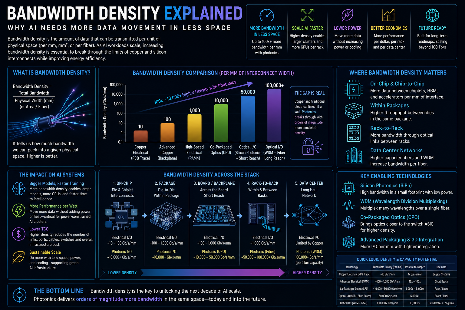
This study graphic summarizes the core bandwidth-density lesson: what bandwidth density means, why AI systems need more data movement in less space, where physical limits appear, and how photonics, WDM, optical I/O, and photonic chiplets help increase throughput across packages, boards, racks, and data centers.
Offer this as a downloadable bandwidth-density study reference.
Connect this form to your email platform and send visitors the full-size Bandwidth Density infographic. This keeps the page educational while turning the visual reference into a useful lead magnet.
Bandwidth density is how much data movement fits into a limited physical boundary.
Bandwidth density is the amount of data throughput available per unit of physical constraint. Depending on the system, that constraint might be chip edge, package shoreline, board area, front-panel space, fiber count, rack footprint, or watts.
AI infrastructure cares about bandwidth density because accelerators, switches, memory, and storage need to exchange enormous data volumes. More compute does not help if the system cannot physically move enough information into and out of the devices.
Bandwidth density is the difference between “we need more bandwidth” and “we need more bandwidth without adding endless pins, cables, traces, power, heat, and space.”
Bandwidth density measures throughput divided by a physical limit.
Bandwidth alone tells you how much data moves. Bandwidth density tells you how efficiently that bandwidth fits into a physical system.
Examples:
Tbps/mm of chip edge
Tbps/mm² of package or chip area
Gbps per fiber
Tbps per rack unit
Gbps per watt
There is no single universal bandwidth-density metric. The right metric depends on the bottleneck being studied.
AI scaling is a bandwidth-density problem.
Large AI systems require high-bandwidth communication between accelerators, memory, switches, storage, and racks. As the number of compute devices grows, the interconnect fabric must scale too.
More accelerators need more links
GPU and XPU clusters create massive east-west traffic between devices and racks.
Data must feed compute
AI workloads need bandwidth between compute, HBM, memory pools, and storage systems.
Fabrics need denser ports
AI switches must move more traffic through limited ASIC, package, and front-panel space.
Electrical scaling runs into pins, traces, connectors, reach, heat, and space.
Electrical interconnects are essential, especially for short-reach and local communication. But as bandwidth rises, the physical layer gets harder. More electrical lanes require more package escape, more routing, more power, more equalization, and more cooling.
Photonics improves bandwidth density by changing the data movement medium.
Photonics moves information with light through fiber or waveguides. This gives system designers new scaling dimensions: optical wavelength, fiber density, optical I/O, silicon photonics, co-packaged optics, and photonic chiplets.
High bandwidth through small media
Fiber can move large throughput without the same distance penalties as high-speed copper.
Optical routing on chips
Integrated photonics routes light through compact chip-scale paths.
Bandwidth near compute
Optical I/O brings high-density optical links closer to packages and accelerators.
WDM lets multiple data channels share one optical path.
Wavelength-division multiplexing is one of the reasons photonics is so powerful for bandwidth density. Multiple wavelengths of light can travel through the same fiber or waveguide, with each wavelength carrying a separate data stream.
λ2 → data channel 2
λ3 → data channel 3
λ4 → data channel 4
More wavelengths = more bandwidth without adding more physical paths.
WDM is not free. It requires wavelength control, filters, multiplexers, demultiplexers, lasers, thermal stability, and calibration. But it gives photonic systems a bandwidth-density lever that copper does not have in the same way.
Bandwidth density becomes a package-level problem.
Advanced AI packages already contain compute dies, memory stacks, interposers, substrates, and high-speed electrical interfaces. The package must move data out without becoming too large, too hot, too expensive, or too hard to route.
Optical I/O and photonic chiplets can help by moving high-bandwidth data through optical channels rather than relying only on electrical package escape.
At AI scale, the problem is not only making the chip faster. It is getting enough data into and out of the chip package.
Bandwidth density depends on which bottleneck you are measuring.
Different engineering teams may use different bandwidth-density metrics because their constraints are different.
| Metric | What It Measures | Why It Matters |
|---|---|---|
| Tbps/mm | Throughput per millimeter of chip edge or shoreline | Important for package escape and chiplet integration. |
| Tbps/mm² | Throughput per area | Important for dense photonic engines and integrated optical receivers. |
| Gbps/fiber | Throughput per fiber | Important for cable count, fiber management, and rack scaling. |
| Gbps/watt | Throughput per unit power | Connects bandwidth density with energy per bit and cooling. |
| Ports per switch | Network connectivity per system | Important for AI fabric size, topology, and scaling. |
| Bandwidth per rack | Total data movement per physical rack footprint | Important for data-center layout, cooling, and system utilization. |
Higher bandwidth density creates new bottlenecks.
Increasing bandwidth density is not just packing more links together. It requires solving power, heat, packaging, signal integrity, manufacturability, and reliability at the same time.
More links can mean more heat
Dense optical and electrical systems need careful thermal design.
Physical cabling becomes complex
High-density optical systems need reliable fiber attach, routing, and serviceability.
Light sources must scale
Laser efficiency, placement, wavelength control, and reliability affect system economics.
Alignment must be precise
Small optical misalignments can create large losses.
Every dense link must be verified
High-volume systems require electrical, optical, thermal, and firmware validation.
Dense systems must last
AI data centers need stable links under heat, load, aging, and maintenance cycles.
The future of AI bandwidth is denser, closer, and more optical.
AI infrastructure will demand more bandwidth through limited physical space. That pushes photonics closer to the silicon through optical interconnects, co-packaged optics, optical I/O, photonic chiplets, silicon photonics, and WDM.
The long-term direction is electronic-photonic integration: electronics for compute and control, photonics for dense data movement across packages, boards, racks, and data centers.
Bandwidth density, explained clearly.
What is bandwidth density?
Bandwidth density measures how much data throughput fits into a physical constraint such as chip edge, package area, fiber count, rack space, or power budget.
Why does bandwidth density matter for AI?
AI systems need enormous communication bandwidth between accelerators, memory, switches, and racks. Physical space for links, cables, pins, and power is limited.
How does photonics improve bandwidth density?
Photonics can move high bandwidth through fiber and waveguides, use wavelength-division multiplexing, and bring optical I/O closer to compute packages.
What is Tbps/mm?
Tbps/mm means terabits per second per millimeter. It is often used to measure throughput along chip edge or package shoreline.
How does WDM help bandwidth density?
WDM sends multiple wavelengths through the same fiber or waveguide, allowing more independent data channels without adding more physical paths.
What limits bandwidth density?
Limits include power, heat, package routing, fiber attach, laser efficiency, coupling loss, reliability, testing, and serviceability.