Photonic Chiplets Explained
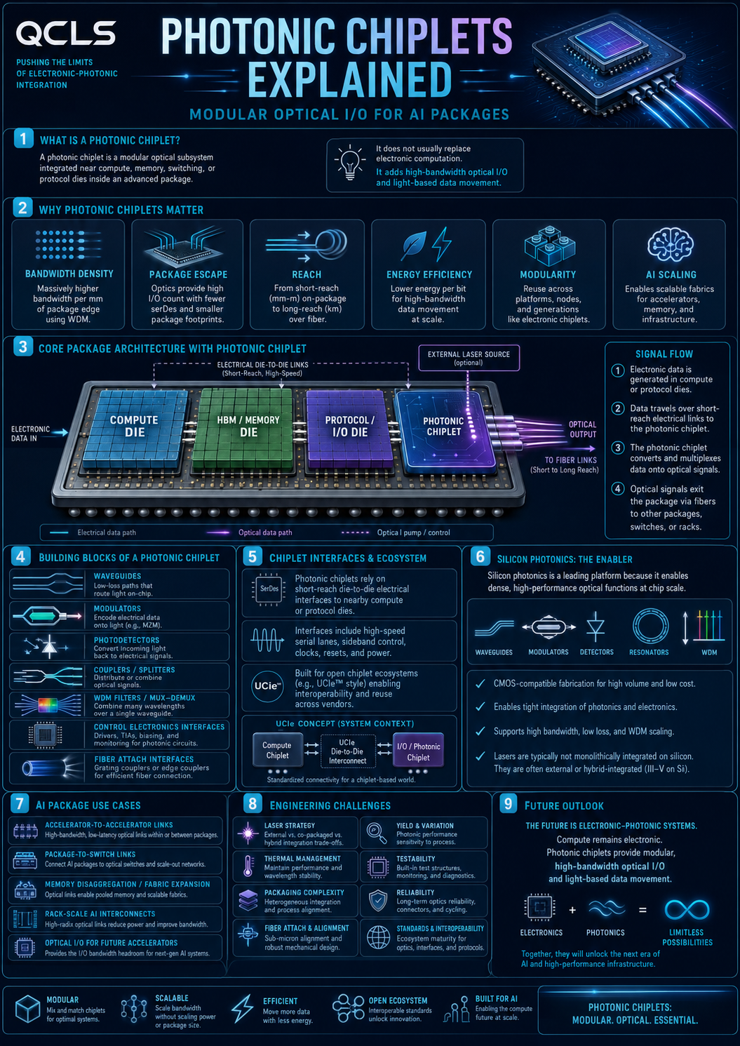
Photonic chiplets are modular optical building blocks that can sit beside compute, memory, switching, or protocol chiplets inside advanced packages. Their job is not to replace electronic computation — it is to give electronic systems a high-bandwidth optical path for moving data with light.
Photonic Chiplets at a Glance
This study graphic summarizes the core photonic chiplet lesson: what photonic chiplets are, why they matter for AI packages, how they connect compute and memory to optical I/O, how silicon photonics enables them, and why modular optical building blocks can help scale future electronic-photonic systems.
Offer this as a downloadable photonic chiplets study reference.
Connect this form to your email platform and send visitors the full-size Photonic Chiplets infographic. This keeps the page educational while turning the visual reference into a useful lead magnet.
Photonic chiplets turn optical I/O into a modular package building block.
A photonic chiplet is a compact optical subsystem designed to be integrated near electronic dies inside an advanced package or module. It can contain silicon photonic circuits, modulators, detectors, couplers, WDM functions, and interfaces to lasers and fibers.
The core idea is modularity. Instead of building a full processor out of photonics, the system can keep computation electronic while adding a photonic chiplet for high-bandwidth data movement. This is especially important for AI accelerators, switch ASICs, chiplet platforms, memory fabrics, and future rack-scale systems.
Photonic chiplets are the bridge between silicon photonics and advanced electronic packaging.
A photonic chiplet is a specialized optical I/O tile.
In a chiplet system, different dies perform different functions. One die might handle compute. Another might handle memory. Another might translate protocols. A photonic chiplet adds optical connectivity to that package.
The photonic chiplet is usually not doing general-purpose computation. It is moving information. It converts electrical data from nearby electronics into optical signals, sends those signals through fiber or waveguides, and receives optical signals from other parts of the system.
AI systems need more bandwidth than electrical packaging can comfortably scale forever.
Advanced AI packages already combine accelerators, memory stacks, interposers, high-speed interfaces, and power delivery. As systems scale, the package has to move enormous amounts of data in and out without wasting power or creating excessive heat.
Optics as a separate tile
Photonic chiplets let designers add optical I/O without making the main compute die photonic.
More data per edge and package area
Optical links and wavelength multiplexing can increase how much data leaves the package.
From package to system scale
Optical paths can connect accelerators, switches, memory pools, and racks over longer distances.
Shorter electrical paths
Keeping high-speed electrical links short can reduce equalization and SerDes pressure.
Separate optical roadmap
Photonic chiplets can evolve alongside compute chiplets and packaging technologies.
New compute fabrics
They enable larger AI fabrics, optical scale-up links, and future disaggregated systems.
A photonic chiplet is part of a complete electro-optical package.
The chiplet itself is only one piece. A working system requires nearby electronic dies, electrical interfaces, laser power, fiber attach, thermal design, control firmware, and system-level reliability.
| Element | Role | Why It Matters |
|---|---|---|
| Compute die | Generates and consumes data | The GPU, accelerator, CPU, XPU, or switch ASIC remains electronic. |
| Die-to-die interface | Moves electrical data to the chiplet | Needs short reach, high bandwidth, low latency, and low power. |
| Photonic chiplet | Converts data into optical signals | Contains optical I/O functions such as modulators, detectors, waveguides, and WDM. |
| Laser source | Provides optical carrier power | May be external, remote, attached, or integrated depending on architecture. |
| Fiber attach | Gets light out of the package | Alignment, loss, reliability, and serviceability define commercial viability. |
| Control electronics | Stabilizes the optical system | Thermal tuning, calibration, monitoring, and fault handling are essential. |
Photonic chiplets need clean electrical interfaces to nearby dies.
For a photonic chiplet to work inside a multi-die package, the nearby electronic dies need a way to communicate with it. That can involve die-to-die interfaces, protocol converters, short-reach electrical links, and open chiplet ecosystems.
The key point is that the optical chiplet does not sit alone. It must receive data from electronic silicon, convert it to light, and fit into a package architecture that chip designers can actually use.
The photonic chiplet is only useful if the electrical interface into it is dense, low-power, low-latency, and package-friendly.
Silicon photonics is one of the main technology platforms for photonic chiplets.
Silicon photonics can build waveguides, modulators, photodetectors, resonators, couplers, filters, and wavelength multiplexing structures on chip-scale platforms. That makes it a strong candidate for optical engines and photonic chiplets.
Silicon is attractive because of semiconductor manufacturing scale and integration potential, but it is not perfect. Laser integration, coupling, thermal drift, insertion loss, and packaging all remain difficult.
Optical paths on chip
Waveguides route light through the photonic chiplet.
Electrical data becomes light
Modulators imprint electronic data onto optical carriers.
Light becomes electrical data
Photodetectors convert received optical signals into electrical signals.
Photonic chiplets can help AI packages communicate beyond the package boundary.
AI accelerators already depend on advanced packaging to integrate compute dies, memory stacks, interposers, high-speed I/O, and power delivery. Photonic chiplets extend that packaging concept into optical connectivity.
Photonic chiplets are powerful because they are integrated — and hard for the same reason.
A credible photonic chiplet system has to solve many problems at once: optical design, electronic interface design, package integration, laser strategy, thermal control, fiber attach, manufacturing, and field reliability.
Light source placement is difficult
Lasers may be remote, external, integrated, or shared, each with different thermal and serviceability trade-offs.
Photonic devices can move with temperature
Microrings, interferometers, and filters can require tuning and calibration.
Getting light out is hard
Low-loss, reliable, high-volume optical coupling is one of the hardest packaging problems.
The short link still matters
The chiplet interface must be dense, low power, low latency, and compatible with package design.
Validation crosses domains
Manufacturing must test electrical, optical, thermal, mechanical, firmware, and system behavior.
Standards and supply chains matter
Broad deployment depends on interoperable chiplet interfaces, foundries, packaging, lasers, and tools.
Photonic chiplets are a building block for future electronic-photonic systems.
The long-term trend is clear: electronics will keep computing, while photonics will increasingly move high-bandwidth data. Photonic chiplets make that division modular.
Future AI packages may combine compute chiplets, HBM, protocol chiplets, photonic I/O chiplets, external laser sources, silicon photonic engines, and optical fibers inside advanced packaging ecosystems.
Photonic chiplets, explained clearly.
What is a photonic chiplet?
A photonic chiplet is a modular optical subsystem that can be integrated near electronic dies to provide optical input/output and high-bandwidth data movement.
Does a photonic chiplet compute with light?
Usually no. Most photonic chiplets are designed for communication and optical I/O, not general-purpose computation.
Why do AI systems need photonic chiplets?
AI packages need massive bandwidth in and out of compute dies. Photonic chiplets can help move data beyond package and board limits with light.
How are photonic chiplets related to optical I/O?
Photonic chiplets are one practical way to implement optical I/O near processors, accelerators, switches, and memory systems.
What technology is used to build photonic chiplets?
Many designs use silicon photonics, often combined with electronic drivers, receivers, lasers, fiber coupling, and advanced packaging.
What are the biggest challenges?
Major challenges include laser strategy, thermal control, coupling loss, fiber attach, testing, standards, serviceability, and manufacturing yield.